Cryogenic Nanoscopy
Cryogenic scanning near-field microscopies

The Challenge: Overcoming the Nanoscale Imaging Barrier in Quantum Materials
Developing next-generation quantum technologies and energy-efficient devices demands an in-depth nanoscale understanding of quantum materials. However, conventional optical instruments face fundamental limits imposed by diffraction, restricting spatial resolution to roughly half the wavelength of the illuminating radiation. This limitation is particularly severe for longer wavelengths such as mid/far-infrared and terahertz (THz) radiation. For instance, THz waves have wavelengths near 300 micrometers, which caps the lateral resolution at about 150 micrometers. Such coarse resolution obscures the nanoscale phenomena that are critical to many quantum materials. Consequently, key quantum properties and correlated electronic behaviors—such as phase separation, domain formation, moiré patterns, and collective modes—remain hidden, slowing the advancement of transformative quantum devices and circuits.
Our Approach: Pioneering Advanced Optical Nanoscopy
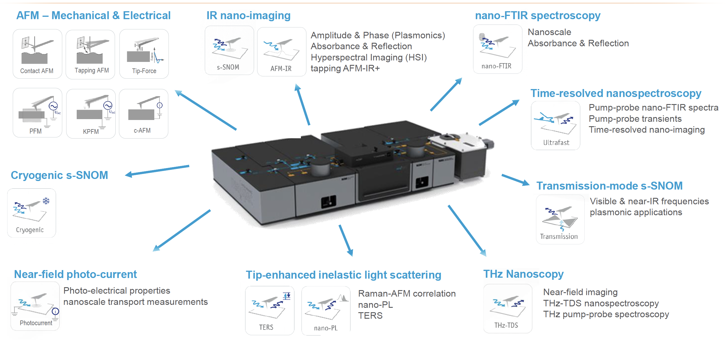
Our research tackles this fundamental barrier by developing and applying cutting-edge optical nanoscopy and nanospectroscopy techniques that break past the diffraction limit. Scattering-type scanning near-field optical microscopy (s-SNOM) presents a powerful solution by surpassing this diffraction limit across a wide spectral range, from visible to THz frequencies. This technique utilizes an atomic force microscope (AFM) with a light-illuminated tip that scans across the sample, collecting elastically scattered light to generate near-field optical images with exceptional spatial resolution of less than 10 nanometers, independent of the illumination wavelength.
The s-SNOM setup incorporates a parabolic mirror for illuminating the tip and collecting elastically scattered radiation. To achieve complete background suppression, a reference beam is phase-modulated using pseudo-heterodyne interferometry. For nanoimaging with monochromatic light sources, the tip-scattered radiation is interfered at the detector with a reference beam reflected at a planar reference mirror, enabling amplitude-resolved and phase-resolved detection. The s-SNOM can also operate with broadband light sources for nanospectroscopy (nano-FTIR), utilizing the Michelson-type interferometer as an asymmetric Fourier transform (FT) spectrometer. Hyperspectral nanoimaging is achieved by recording spectra at each pixel on a sample’s surface, generating data cubes from which local spectra or monochromatic images can be extracted.
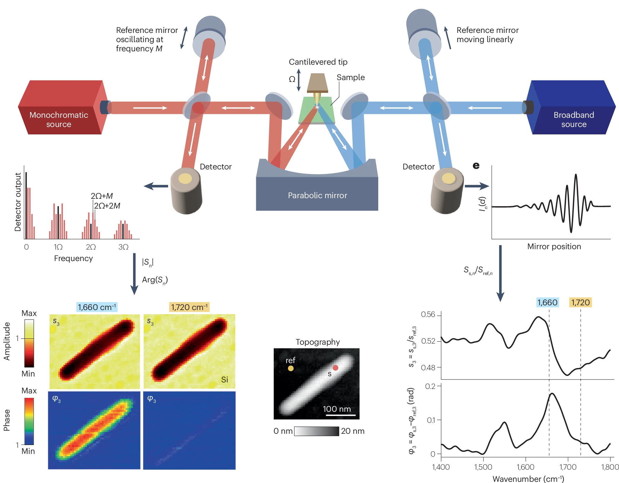
We integrate s-SNOM technology with advanced functionalities—including a cryogenic stage, controllable electric and magnetic fields, and visible-to-THz laser sources—to realize correlative cryogenic nanoscopy for comprehensive analysis of material properties across diverse length, frequency, and energy scales. This platform can simultaneously measure multiple properties over a wide temperature range while maintaining high optical spatial resolution within a single instrument, addressing key challenges associated with slow, costly nanoscale measurements and difficult cross-technique data correlation.
Strong light-matter interactions in 2D materials
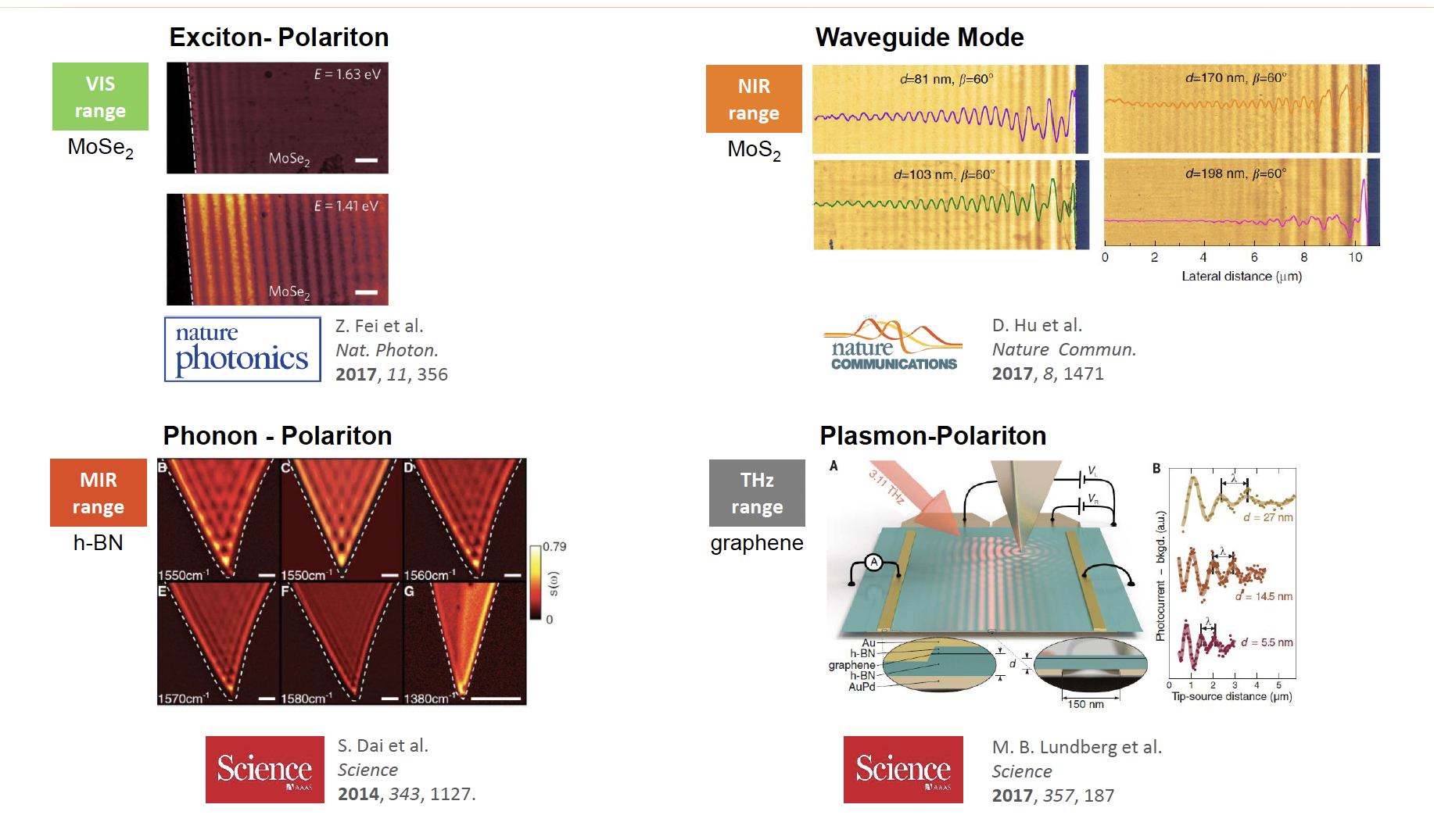
Another research direction focuses on the confinement and control of light at the nanoscale. The low dimensionality and strong correlations in 2D quantum systems give rise to rich electronic and structural properties that manifest as collective excitations—such as plasmons in metals, excitons in semiconductors, phonons in polar dielectrics, magnons in (anti)ferromagnets, and Cooper pairs in superconductors. When these excitations couple strongly to photons, they form tightly confined light–matter hybrid modes known as polaritons, which span a broad region of the electromagnetic spectrum from microwave to ultraviolet wavelengths and offer unprecedented optical field confinement.
A central challenge in imaging and spectroscopically probing polaritons is their large momentum mismatch with free-space photons. The strongly confined near field of s-SNOM provides the required large momentum to launch and visualize polaritonic waves as they propagate along a material’s surface, revealing key insights into correlated and topological quantum phenomena in the underlying host materials.
In addition to s-SNOM, we actively investigate emerging materials using a broad suite of scanning probe microscopy techniques, including photo-induced force microscopy (PiFM), AFM-based infrared spectroscopy (AFM-IR), piezoresponse force microscopy (PFM), magnetic force microscopy (MFM), Kelvin probe force microscopy (KPFM), and scanning tunneling microscopy (STM).
Impact and Discoveries
These unique experimental tools have enabled us to uncover rich nanoscale behaviors in a wide range of quantum materials, including emergent ferroelastic phases (Nature Materials 2018; Nature Communications 2020; Science Advances 2022; Nature Communications 2022), ferroelectric phases (ACS Nano 2023; Nature Communications 2022; Advanced Science 2021; Nano Letters 2019), and magnetic phases (Advanced Materials 2019; JACS 2023), as well as superconducting transitions (ACS Nano 2018), highly ordered porosity (Nature Chemistry 2017), and complex stoichiometric phases (Advanced Materials Interfaces 2018). We also investigate the formation of new chemical bonds (Desalination 2019), optical phonon modes (Advanced Materials 2018), and plasmon–phonon polaritons (ACS Materials Letters 2021) at a variety of interfaces and nanostructures. By directly visualizing and controlling these emergent quantum phenomena, we are helping to lay the groundwork for future AI hardware, quantum computing platforms, and related technologies.
Van der Waals materials & devices

Sustainable AI & Quantum Hardware

Facilities
