Sustainable AI & Quantum Hardware
Enabling Energy-Efficient Devices for Neuromorphic and Quantum Photonic Computing
By pushing the frontiers of optical nanoscopy and leveraging quantum materials, our research aims to reveal and control quantum phases and excitations at the nanoscale, enabling transformative advances in neuromorphic computing, quantum information hardware, and energy technologies.

1. Ultra-Low-Power Electronics
The Challenge: Energy-Hungry AI and the Limits of Conventional Architectures
The exponential rise of AI is driving computing-related electricity demand toward a projected ~25% of global usage by 2030—a trajectory that is both economically and environmentally unsustainable. A dramatic reduction in energy per operation (by orders of magnitude) will require moving beyond conventional Boolean logic and von Neumann architectures toward neuromorphic computing, as well as developing new classes of spin–orbit torque (SOT) devices.
Both of these pathways rely heavily on quantum materials—systems in which strongly correlated phenomena such as magnetism, ferroelectricity, multiferroicity, superconductivity, and nontrivial band topology naturally emerge.
Materials and Devices for Neuromorphic Computing
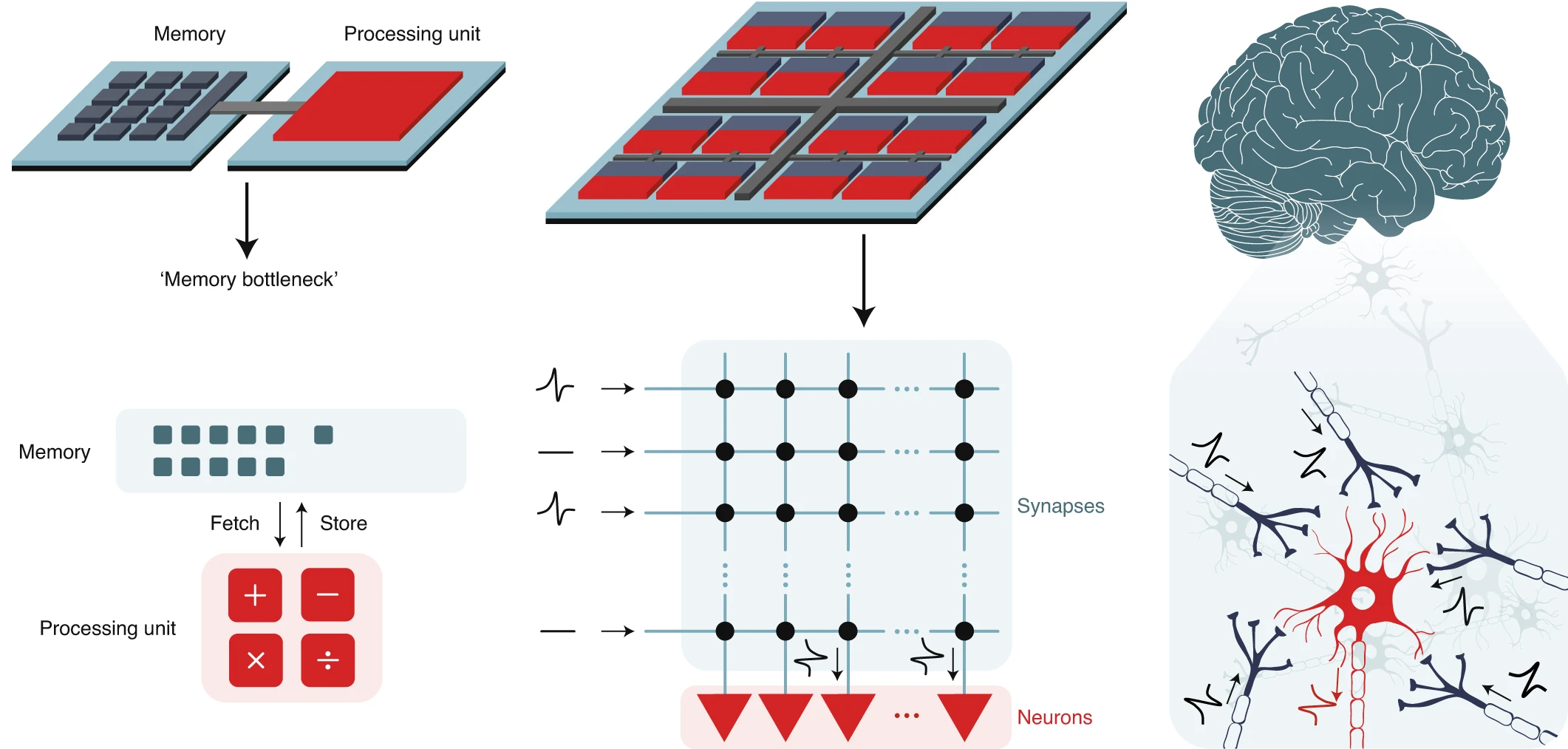
Modern computers are built on the von Neumann architecture, where memory and processing are physically separated. Data must be continuously shuttled between memory and the processor, and the rate at which this can be done—the so‑called memory wall—sets a fundamental performance and energy bottleneck. If the energy per operation in today’s computers (on the order of ~100 pJ/operation) is not reduced, the rapid growth of microelectronic components driven by the Internet of Things and AI/ML will cause microelectronics to account for a substantial fraction of global energy consumption.
Neuromorphic computing seeks brain-inspired devices and architectures that can deliver highly energy-efficient hardware for AI. At the device level, this requires:
- Merging memory and logic to enable compute-in-memory architectures, and
- Memristive behavior that mimics synapses and neurons, with threshold-like switching and a wide range of programmable, non-volatile resistance states.
Our Approach:
We engineer quantum materials and devices that mimic neural architectures by merging memory and logic at the nanoscale, enabling brain-inspired, energy-efficient compute‑in‑memory hardware. Our research spans novel ferroelectric, spintronic, and nonlinear optical materials (e.g., Advanced Functional Materials 2020; Advanced Materials 2019) to realize artificial neurons and synapses that exhibit:
- Analog and multilevel switching
- Nonvolatility
- Ultralow energy operation
- Network-scale addressability
These neuromorphic platforms have the potential to reduce energy consumption by several orders of magnitude, paving the way for next‑generation hardware for AI.
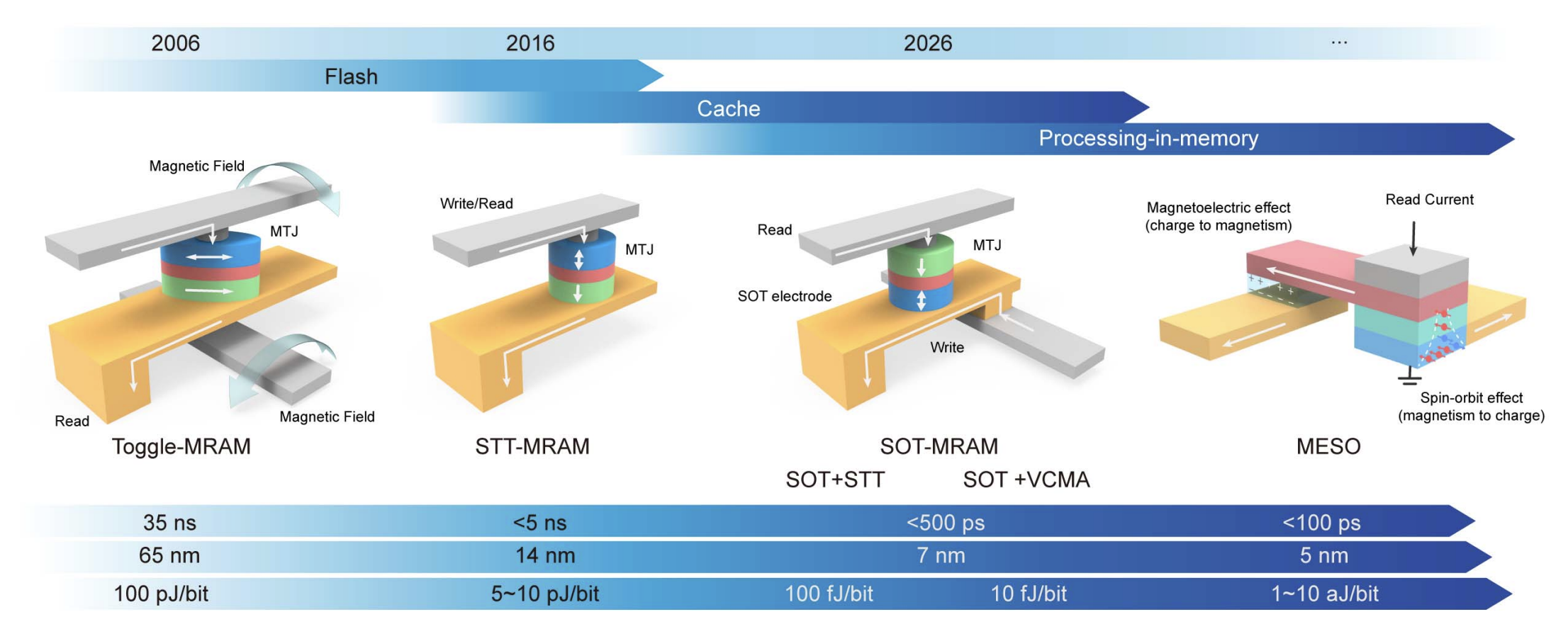
Spin–Orbit Torque Devices
Electric-field control of magnetism in spin–orbit torque (SOT) memory devices and magnetoelectric spin–orbit (MESO) memory–logic devices offers a promising route to ultra‑low‑power electronics, with target energies in the femtojoule (SOT) to attojoule (MESO) range per operation. In these devices, an SOT electrode converts charge current into spin current, which flows into an adjacent magnetic layer and exerts a torque that switches its magnetization—an essential process for next-generation memory and logic.
However, in most conventional SOT materials, such as heavy metals and topological insulators, high crystal symmetry constrains the spin polarization to lie predominantly in the plane of the material. This limitation often necessitates an external magnetic field to achieve deterministic magnetization switching, complicating device design and increasing energy cost.
Our Approach:
We have shown that low-symmetry crystals—such as monoclinic and triclinic chiral 2D perovskites (Science 2024)—generate spin currents with components along multiple directions, including out-of-plane orientations that are inaccessible in standard SOT materials. This anisotropic spin texture enables field-free switching, eliminating the need for an external magnetic field to switch the magnetic state.
In chiral 2D perovskites, we have demonstrated:
- High SOT efficiency (~5%) at room temperature, enabling more energy-efficient switching
- Solution-based synthesis below 100 °C, in stark contrast to many advanced materials that require expensive, high-temperature, ultrahigh-vacuum growth
These characteristics translate into simpler, lower-power devices that are easier to scale—impacting everything from energy-intensive data centers to battery‑constrained edge devices such as wearables and sensors.
Our ongoing research focuses on discovering and optimizing novel low-symmetry quantum materials that combine high SOT efficiency, low cost, scalable synthesis, and robust performance, unlocking powerful spin currents and new ways to control magnetism at the atomic scale for smarter, more sustainable electronics.
2. Photonic Integrated Circuits
The ability to modulate light propagation in a material using external stimuli is essential for a wide range of photonic applications, from optical interconnects and pulse generation to biosensing and medical technologies. Modulation can be driven by various stimuli—optical, electric, or magnetic fields, as well as sound, temperature, and mechanical stress—giving rise to all‑optical, electro‑optic, magneto‑optic, acousto‑optic, thermo‑optic, and mechano‑optic effects. Key performance metrics for any optical modulator include modulation speed, modulation depth, insertion loss, and power consumption.
Today’s dominant approach, electro‑optic modulation, faces fundamental challenges in speed, energy efficiency, and cross‑talk, making it less suitable for applications requiring ultrafast, low‑power operation (e.g., high‑speed data transmission and on‑chip photonic computing).
Our Approach: All‑Optical Modulation with 2D Materials
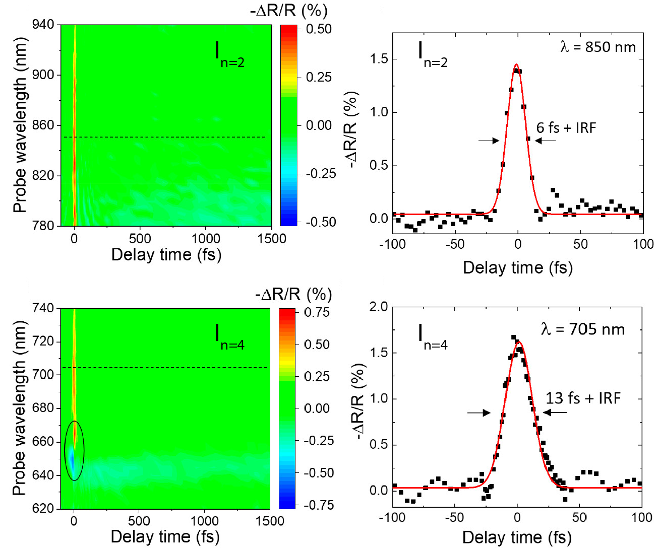
As an alternative, purely nonlinear all‑optical modulation offers intrinsic advantages in terms of ultrafast operation and reduced heat generation. In this scheme, an intense “switching” pulse induces nonlinear optical effects—such as nonlinear absorption and nonlinear refraction—in the material, thereby controlling the propagation of a second, lower‑power “signal” pulse. The switching beam modifies the material’s complex refractive index by generating a non‑equilibrium carrier population that relaxes on ultrafast (typically femtosecond) timescales. This enables signal processing fully in the photonic domain, with modulation speeds well beyond 100 GHz, and opens pathways for high‑bandwidth applications including on‑chip interconnects, fiber‑to‑the‑home links, astronomical imaging, and advanced medical diagnostics.
We investigate all‑optical modulation in 2D materials with exceptionally large nonlinear optical responses (ACS Nano 2019; ACS Nano 2021; Nature Communications 2020). For example, under sub‑bandgap excitation, 100‑nm‑thick perovskite sheets enable ultrafast all‑optical modulation within a 20‑fs window via the optical Kerr effect and two‑photon absorption, corresponding to potential modulation speeds exceeding 50 THz. This demonstrates that nonlinear 2D materials are promising candidates for nanoscale all‑optical modulators in the visible and near‑infrared, with applications in ultrafast information processing, optical data transmission, and high‑performance computing.
More broadly, 2D materials offer key advantages for optoelectronic and photonic technologies, especially outside the spectral range accessible to silicon. Their direct band gaps make many semiconducting 2D materials attractive for efficient light emission, while semi‑metallic and small‑band‑gap systems such as graphene and black phosphorus (ACS Photonics 2018) extend device operation deep into the infrared, where they can compete with—and complement—conventional, often costly III–V semiconductor platforms.
3. Quantum Technologies
Quantum networking and distributed quantum sensing rely on photonic links—“flying qubits”—to connect nodes and enable scalability over large distances and complex network topologies. In the simplest case, an interconnect consists of a photon traveling from one node to another, with both nodes operating at the same wavelength. In heterogeneous networks, however, different nodes perform different functions at different wavelengths, and more sophisticated interconnects are required.
To connect two nodes operating at different wavelengths, two primary strategies are used:
- Quantum frequency conversion (QFC) / quantum transduction, which converts the wavelength of a photon emitted by one node to that of the other node; and
- Entangled photon pair sources, in which the two photons have wavelengths matched to the two different nodes.
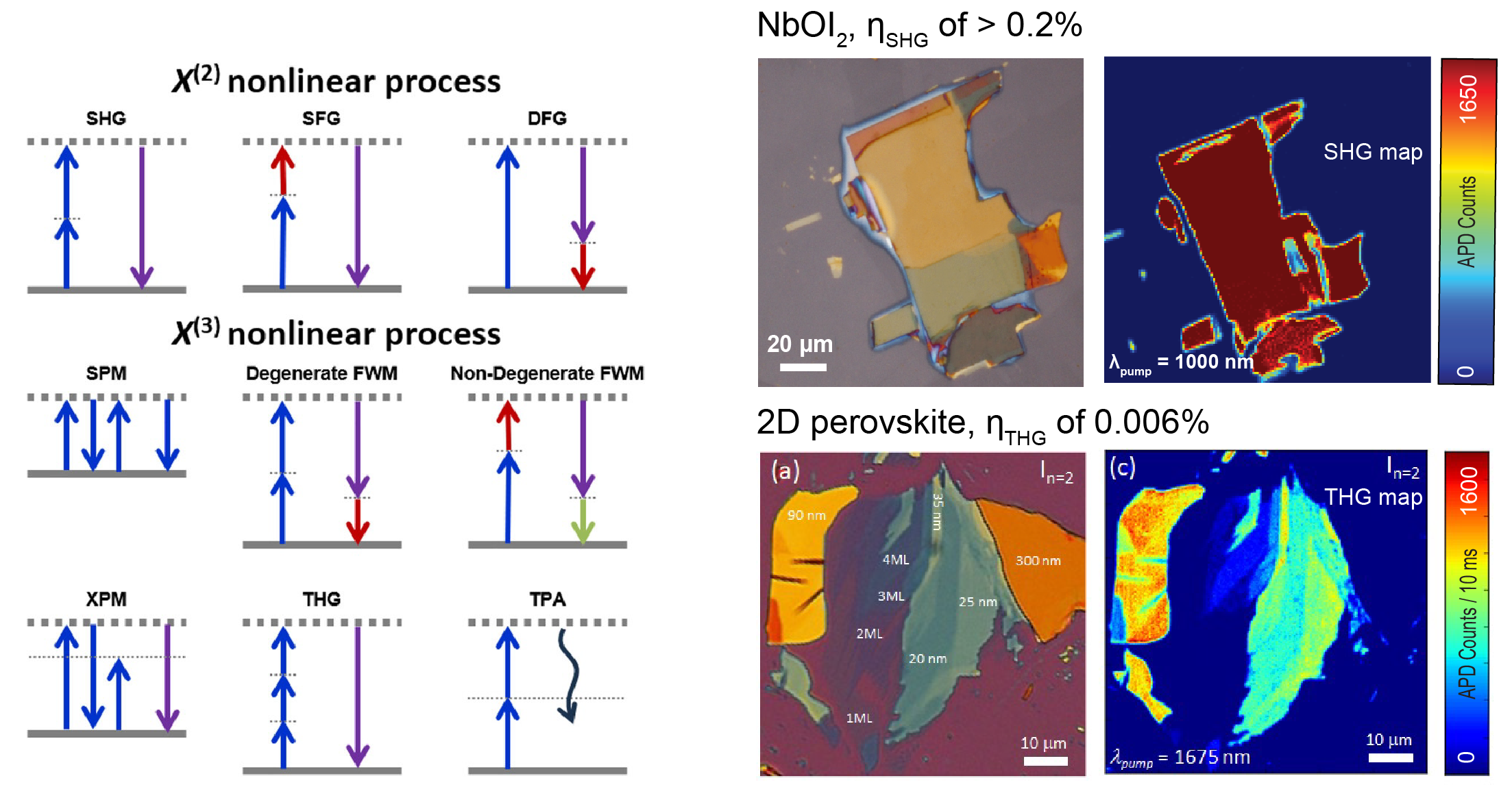
Both approaches fundamentally rely on nonlinear optical processes.
However, in conventional nonlinear materials, photon–photon interactions are intrinsically weak. Achieving appreciable nonlinear responses typically requires high-intensity pump beams, large interaction volumes, and stringent phase-matching techniques. These constraints make it challenging to design miniature, integrated quantum devices—such as sources, interfaces, and memories—that operate efficiently at moderate input powers.
Our Approach:
To overcome these limitations, we harness 2D quantum materials with unique order parameters (e.g., polar order and collective excitonic excitations) as well as artificially engineered metasurfaces to induce strong second- and third-order nonlinear interactions at the nanoscale (Advanced Optical Materials 2023; Nature Photonics 2022; ACS Nano 2021; Advanced Materials 2019; Advanced Materials 2019; ACS Nano 2018; ACS Photonics 2018; JACS 2017). In these systems, light waves interacting with atomically thin sheets can strongly couple to one another and exhibit enhanced nonlinear responses, enabling processes such as:
- Second-harmonic generation (SHG)
- Sum-frequency generation (SFG)
- Spontaneous parametric down-conversion (SPDC)
- Self-phase modulation (SPM)
- Third-harmonic generation (THG)
- Two-photon absorption (TPA)
- Four-wave mixing (FWM)
Crucially, these effects can be realized in compact geometries without stringent phase-matching constraints, opening a pathway to truly nanoscale nonlinear photonics.
By exploiting the large optical nonlinearities of layered quantum materials and metasurfaces, our work establishes a promising platform for next-generation, integrated, high-fidelity quantum communication and networking components.
Van der Waals materials & devices

Cryogenic Nanoscopy

Facilities
